All Flex Flexible Printed Circuits and Assemblies
Founded in 1977, All Flex Solutions is a leading provider of specialty flex and rigid flex printed circuits, flexible heaters, and value-added assemblies for mission- and life-critical applications. All Flex products can be found in many applications and markets, including medical, defense, aerospace, semiconductor, industrial and telecommunications.
Our Products

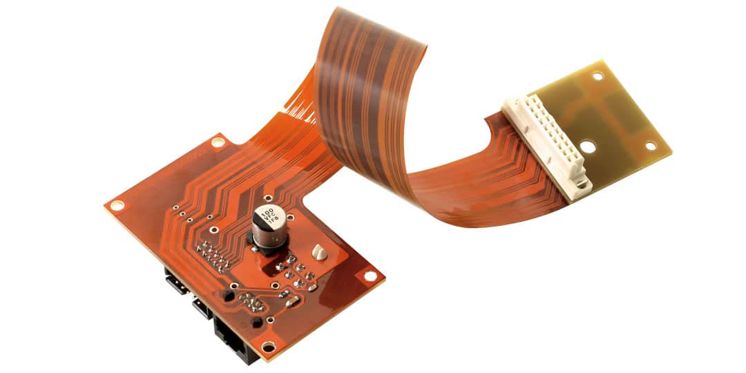
Flexible Printed Circuits Solutions
Flexible printed circuits can be bent and configured in just about any shape or thickness; creating tremendous options when designing an electronics package.

CatheterFlex™ Solutions
CatheterFlex™ circuits eliminate the need for wires, greatly simplifying the entire manufacturing process for catheters that are used to diagnose and treat medical conditions.

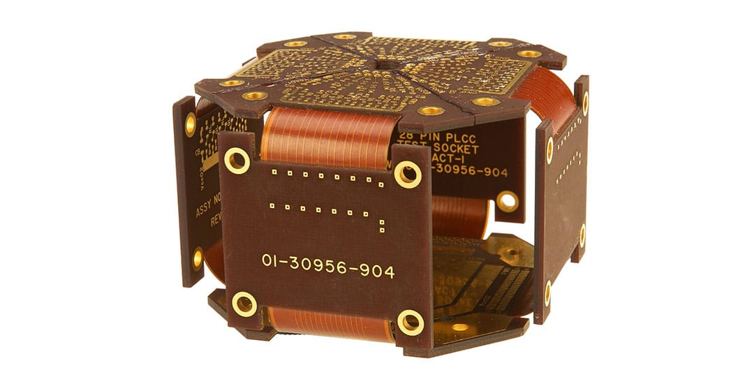
Rigid Flex Solutions
The ultimate electronic packaging solution that provides you with high-density circuit routing in a foldable format that is very reliable in challenging environments.

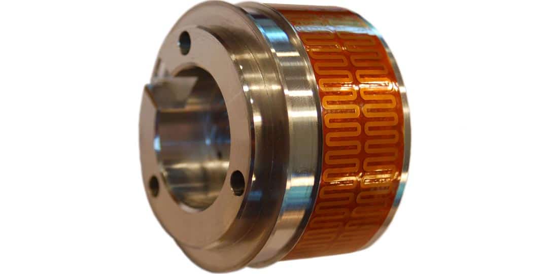
Heater Solutions
AllFlex provides highly customized polyimide and silicone rubber heaters that are engineered specifically to meet the overall physical, thermal and environmental requirements of each design.
The All Flex Engineering Staff Has An Experiential Edge That Can’t Be Beat
All Flex engineers have significant experience in the flexible printed circuit, flexible heater, and rigid flex industries. Whether you are a novice in the area of flexible circuit design or a long time user, we lend our expertise providing comprehensive support from concept to completion.
Industries We Serve

Medical
Today’s medical devices need to be smaller with greater functionality than ever. To meet this demand for miniaturization, medical device manufacturers need to package their electronics to fit within a small form factor. All Flex’s technology provides the perfect solution to this challenge in applications where precision is critical.

Military/Defense
Military electronic devices have unique reliability, dependability, and survivability requirements in addition to strict performance standards. Rigid flex and flex circuits enable defense contractors to meet these demands, helping them produce lightweight military equipment without sacrificing functionality and ultimate never fail reliability.

Aerospace/Aeronautical
Aero electronics systems are exposed to higher levels of shock and vibration while simultaneously evolving toward weight reduction, increased component density and improved functionality. To meet these demands, AllFlex provides aerospace manufacturers with a packaging solution that offers higher reliability and greater survivability without undermining performance.

Analytical/Laboratory
For many analytical tests to be accurate, repeatable and reliable, the test samples need to be at consistent temperatures to eliminate any variability from one sample to the next. All Flex heaters are used to precisely bring samples to defined temperature parameters for these tests to be successfully completed.

General Electronics
We see greater use of flexible and rigid flex circuits and flexible heaters in applications where innovative packaging solutions are required to provide device functionality, miniaturization and reliability. Examples include unmanned vehicles, wearable electronics, robotics, ruggedized computers, solid state disk drives and camera/optics applications.