The circuit traces of a flexible PCB often needs a dielectric covering to selectively protect the traces from shorting against a conductive surface or to prevent select areas from subsequent metal coating or plating operations. The dielectric will have openings that are aligned to specific features of the flexible circuit such as a component pad. This dielectric covering is normally referred to as a coverlay, cover coat or solder mask.
There are a variety of materials and methods that can be used to create this dielectric, criteria for selecting the best options include cost, registration accuracy, environmental requirements, copper thickness and post processing requirements.
The most common types of coverings are:
- Selectively screen printed cover coat
- Pre-punched or drilled dielectric film
- Photo imaged solder mask
- Laser skiving
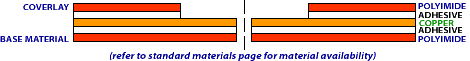
Pre-punched or pre-drilled dielectric film is probably the most versatile method for coverlay creation as while it is more labor intensive than other methods, it can be used in virtually any circuit configuration. The dielectric film is usually polyimide and is coated on one side with a heat activated adhesive. Holes are formed in the dielectric by either drilling or die stamping. The punched coverlay is registered to the substrate and bonded by a heated platen press. A conforming material is usually placed over the assembled substrate while heat and pressure are applied to help insure the coverlay adequately encapsulates the copper.
Photo imageable coverlay or solder mask is often used for high density circuitry or when unusual shapes are needed for the dielectric openings. The photo imageable material is either applied as a liquid coating or as a film that is laminated onto the copper circuitry. The openings are created by exposing selected areas to a high intensity UV light and developing the openings (i.e. the material covering the pad is washed away by a developing chemical). Photo imageable material may not be suitable for 2 oz and thicker copper as it is difficult to achieve conformance to the topography of the circuit traces.
Laser skiving is used where extreme accuracy and tolerance is needed. A dielectric film is bonded over the circuit traces as a solid layer. A laser beam selectively burns the dielectric away while leaving the copper trace undamaged. A secondary cleaning or etching operation is needed to remove the charred residue and oxides created by the laser beam. This is the most expensive method as laser skiving equipment and operation cost are high and the process is more time consuming than the other methods.
All Flex has the capability to use a variety of coverlay systems. You can get more information on All Flex’s capability by visiting its coverlay options section.